Store data from PL (ADC) to PS via DMA in ZCU111

Hi there!

I am Jorge. I am currently developing software/hardware with the ZCU111 board. I am using PYNQ version 2.7.

My goal is the following:
I am acquiring an RF signal through the ADC on the PL and I want to receive it on the PS. For this, I have used the following schematic:

SCHEMATIC:

AXI DMA block config:

Subset Converter block config:

FIFO block config:

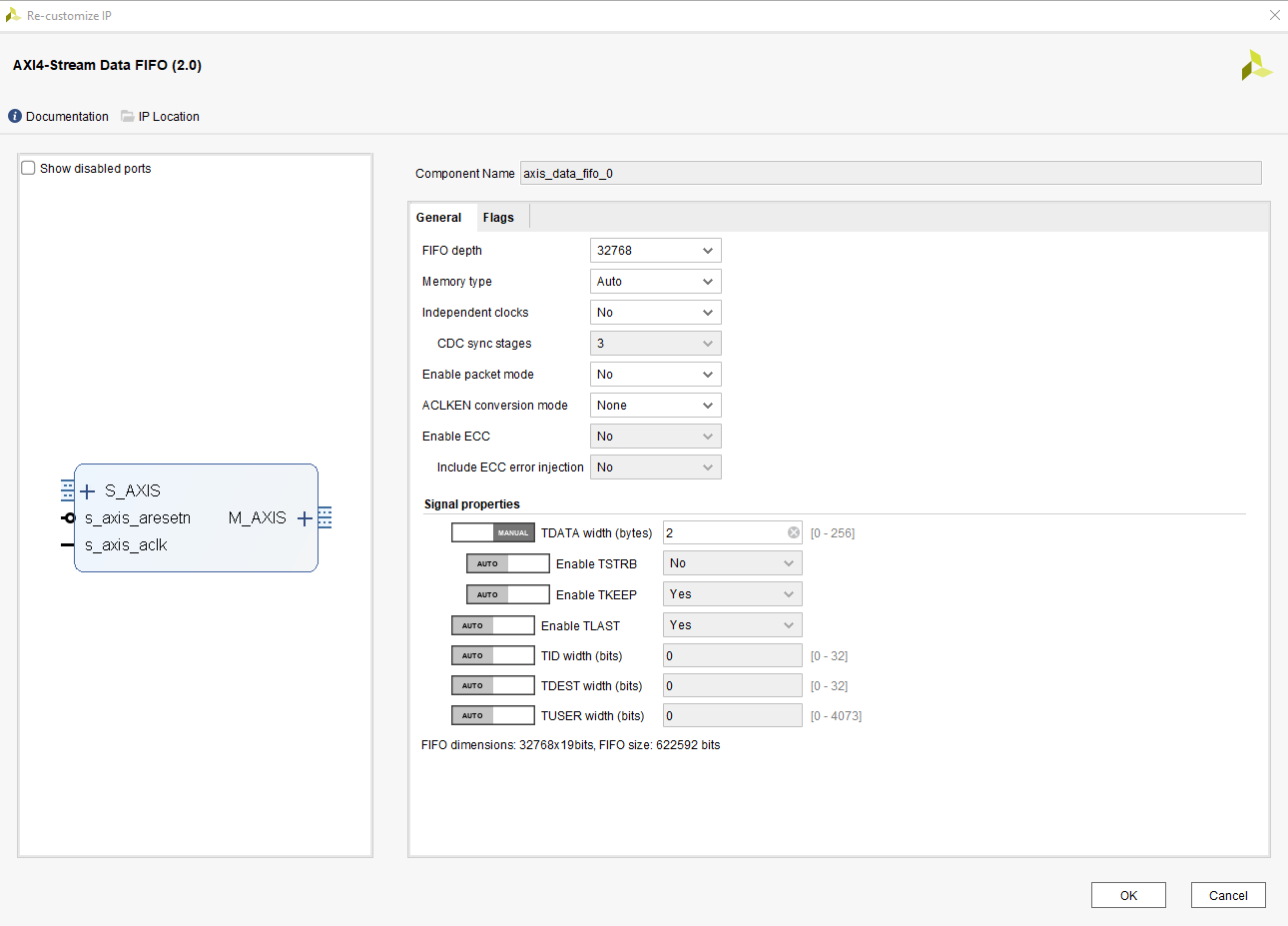
At the moment, I am only using one channel. The RF Data Converter acquires the signal which is real and 16 bits wide, the mixer is in ‘bypassed’ mode, I use a decimation of 8 samples and ejects 1 sample in each clock cycle, which means that the necessary clock is 153.6 MHz since a reference clock of 1228.8 MHz (sample rate = 1228.8 MSPS) is being used.

To achieve my goal I followed the steps of @cathalmccabe during his DMA tutorial and it worked successfully, the problem comes when I try to store the data acquired by the ADC.

Reading in many blogs and topics of this support, I have noticed that the RF Data Converter does not send the TLAST signal needed by the DMA. That is why in the design shown above I use the ‘Subset Converter’ block that generates the TLAST signal every 256 cycles. The signal is then fed into a FIFO that has a depth of 32768 samples and finally reaches the DMA block. Now I am going to show you the error that I suffer in Jupyter:

CODE:

RESULT:

Signal corrupted (after sample 32768):

As you can see, I am receiving a 100 kHz sine wave that looks correct up to sample 32768. This leads me to think that the FIFO is being filled and subsequently the signal is corrupted. Subsequently the signal is being acquired correctly in the PS in 256-sample spans.

I had also tried three other possibilities:

  1. Without using FIFO and without using the ‘Subset Converter’ block:
    In this case, the DMA is able to collect the maximum amount of samples allowed (67108863 bytes) but since it does not receive the TLAST signal, the process gets stuck in the ‘wait()’ function and I cannot make a data request to the DMA again because ‘the DMA is not idle’.

  2. Without using FIFO but using the ‘Subset Converter’ block:
    In this case, the DMA does receive the TLAST signal but nevertheless, in each of the iterations in which a write to the PS memory is requested by the DMA there is a loss of samples (I suppose due to the delay caused in each write) very similar to the one seen in the previous image (in the section after the first 32768 samples).

  3. Using the ‘tlast generator’ block of the XILINX reference design:
    But I have not managed to make it work properly as I get the same result as in auxiliary possibility 1.

How could I manage to store in the PS an amount of samples defined by the buffer size? That is, I want to be able to store X samples in the PS continuously. It is not a problem if between two write iterations by the DMA in the PS there is a small delay causing a phase error.

Thank you very much for your time, I hope you can help me,
Jorge.

1 Like

Hi @ij0r,

I think your original approach is correct. What it could be happening is that the overhead of configuring DMA transactions of 256 samples is larger than the actual transmission time, so the FIFO gets full and you lose samples. It should only take 32 clock cycles to perform this DMA transfer.

I would suggest you increase the number of samples you are sending to the PS, so that the overhead is smaller than the transaction time. Given that the subset converter is limited to generate TLAST every 256 samples (max value), you can add a data width converter before it to pack 8 samples per AXI4-Stream transaction. Alternatively, you can write your own HLS module that generates the TLAST signal.

Mario

Hi @marioruiz,

First of all, thank you very much for your quick reply. I think I understand your explanation. What you mean is that it was sending 16 bit samples and therefore, as the DMA sends 256 “packets” of data in each transaction it was taking too long and causing the FIFO to fill up. So, using the “data width converter” block we are able to send in parallel 8 samples in this case (128 bits) and therefore we make the FIFO not to fill up.

Here is the new schematic with the most important settings as before:

SCHEMATIC:

Data Width Converter block config:

FIFO block config:

Subset Converter block config:

DMA block config:

I have modified the code a bit so that now the buffer is adapted to the maximum size that the DMA writes in memory such that:

CODE:

RESULT:

As you can see, now the signal starts to be corrupted from sample 262220 approx. Can you think what could be happening? Or else, can you try to tell me if I had understood you correctly or if you can clarify it for me.

Thank you very much again,
Jorge

Yes, you got it.

This topic is a bit outside of the scope of this forum. However, I can suggest a few more things

  1. Add more storage, more FIFOs in the path
  2. Use a clock with faster frequency from the DMA to the PS, for instance 200 MHz. Make sure to use proper clock domain crossing.
  3. Try bigger packets, assert TLAST every 4K or 8K transactions.
  4. You may want to profile the copy of buffer to frame. You could try to write directly to frame to remove any copy overhead.

At the end of the day, if the consumer (path from DMA to PS) is slightly slower than the producer (path from ADC to DMA) the FIFO will fill up at some point, so realistically option 2 should be your solution. However, optimizing transactions both in the hw and sw should help as well.

If none of these work, you may need to do lower level debugging to find out where the bottleneck is.

Mario

1 Like

Hi @marioruiz,

Throughout the day today I have been doing numerous tests, of the possibilities you have given me I also think that the only valid one is the 2. This way I think I would get the FIFO to empty faster than it fills and then I would achieve my purpose. Tomorrow I will continue to investigate to realize this solution since I have not succeeded so far.

Otherwise, I think another possibility would be to generate a TLAST with its own block as you told me, being generated this signal (TLAST) when a large number of samples have passed (the one I decide I need for the project). Between different DMA transactions it would have phase jumps but maybe it would be enough.

Many thanks again, we are in touch,
Jorge.

PS: as you said maybe this topic is a bit out of place in the forum but I thank you very much for your help and advice. For this, I have also made a post in the Xilinx support forum.

2 Likes

Hi @ij0r,

What problem did you find using another clock domain? At a high level, you need to:

  1. Enable a second clock in the PS @ 200 MHz
  2. Configure the FIFO to use Independent Clocks
  3. Connect the new clock to the m_axis_aclk in the FIFO, this port and associated reset will appear after you do step 2.
  4. Reconnect clocks and resets of the IP that are after the FIFO to the new domain
  5. Rebuild

Hi again @marioruiz!

I followed your steps but I don’t know if I did them right because it’s as if the new clock domain after the FIFO doesn’t work. I come to this conclusion because the FIFO fills up at the same point or the bottleneck is not there.

Here is the new schematic with the new clock connections highlighted.

I tried with two differents clocks: @200 MHz, @300 MHz and the result is the same, something that I can’t understand. I keep trying, I leave attached my jupyter notebook and also the result with these attempts.


notebook.ipynb (407.1 KB)

Yes, this is not what I would have expected.

You can do further decimation in the PL as you are oversampling so perhaps you can try with x4, or x8.

I have an intuition that the FIFO gets full even before you start the DMA transfers. So, samples are dropped regardless. You may need some logic that controls when data is pushed to the FIFO.

1 Like

Hi @ij0r ,
did you solve the problem? i have the same question
Thanks

@ij0r could you please post your tcl so that we can accurately recreate the design?
Thank you,
Dimitris

Hello again!

First of all, sorry for my tardiness in returning to the thread to comment on my current status. Between the Christmas vacations and the big job I’ve had I had completely forgotten about it.

Finally, I decided to use a block I created myself that takes care of counting samples and generating a TLAST signal. That number of samples that counts will be the one that from the Python environment (PS) we ask to the DMA (PL). A good idea would be that this block has an input so that we can modify the number of samples to count from Python without having to indicate it from VHDL and compiling the .bit every time we want to change it.

In addition an appreciation to consider is that whenever we make a DMA transaction, in the FIFO there will be a number of samples (equal to its depth) that we will have to discard since those samples will have been stored previously and the FIFO is only emptied when the DMA makes the request of X samples. Let’s imagine that the FIFO has a depth of 8192 samples, in that case if we request 65536, only the last 57344 samples will be valid. This is important in my case because the acquisition must be a continuous signal in which there are no phase jumps or time lags.

I hope to help you and sorry for the wait.

3 Likes

Hi @ij0r I am also interested in this application. Would you be able to share the project so that I can recreate the design? Also, what is the maximum sampling rate you are getting from the ADC with this design?