ZCU216 Gen3 RF Design with only LMK DAC230 245.76Mhz ref clk from LMK04828B in CLK140

Hello,

Resorting to help after a month or so of learning curve :sweat_smile:

I’m trying to use the recently released PYNQ 2.7 image for the ZCU216 (here).

I’ve read through plenty of documentation on the examples and the CLK104. Namely this, this, and this.

From what I understand, the B2 and B3 pins on the LPA connector pinout (here) correspond to the E5 and E6 pins on the RFSoC, which in turn can be pulled in to the “dac2_clk” signal, which is associated with the DAC230 tile, correct?

I’d like to use only this reference clock (and not the SSMP cables), to drive the RF Data Converter. Is this possible? (According to the example here which uses only the LMK reference clock for the DACs/ADCs, I understand that it is).

Want I want to do (for now) is very simple: send out a constant tone through DAC230 (which is Tile 2 on the ZCU216 Gen3, I think).
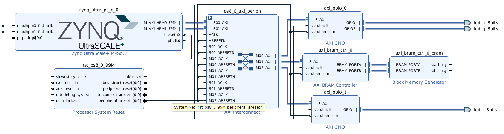
My design:

My RFDC DAC230 and clocking config:

PL Clock is 100Mhz coming from the PS system. Design validation returns no errors. The bitstream generated without errors, and the dac2_clk pins are bound to the E5 and E6 I/Os:

I already have the SDcard booting with PYNQ 2.7 (I’ve tested other example overlays with simple I/O, or even the DMA loopback example, that all works fine). I scp my overlay and hwh into the board, change to root with “su -”, and call python (the bundled version is 3.8).

Following I do:

>>> import xrfclk
>>> import xrfdc
library loaded!
xrfclk.set_ref_clks(245.76)

Using an oscilloscope, I can check the OUTPUT_REF SMA on the CLK104 and see the 7.68Mhz clock being generated after this call. I’m assuming that as this point, the dac2_clk clock is at 245.76MHz (as per example 1 here).

At this point there are few doubts:

  • Are the values of the DAC_REFCLK and ADC_REFCLK actually 245.76Mhz? (These are the outputs labeled DOut6 and DOut12 in the CLK104 documentation)
  • What is the value of PL_CLK? Do I need to pull into the FPGA? What for and how?
  • What is the value of PL_SYSREF? Do I need to pull into the FPGA? What for and how?
  • What is the purpose of the CLK_SPI_MUX_SEL0 and CLK_SPI_MUX_SEL1 pins (which I can control using GPIO from the FPGA). Are they required? Other example designs I’ve seen do not use them. Do I need to set this these pins to 0b’01 to select the 10MHz oscillator (U4) on the CLK104, or is this selection controlled via SPI (and therefore using the xrfclk library when calling set_ref_clks).

Regardless, I can invoke the Overlay function (btw, the question mark operator on the overlay returns a syntax error from the Python interpreter with any overlay I use, help?). I do a quick test on the LEDs to make sure I can change the values, which I can.

Then:

>>> ol = Overlay("/home/xilinx/overlays/ex2v2/mpsoc_preset.bit", ignore_version=True)
>>> ol? # :(
  File "<stdin>", line 1
    ol?
      ^
SyntaxError: invalid syntax 
>>> leds = ol.axi_gpio_0.channel1
>>> leds.write(45645, 0xfffffffff) # leds work :)
>>> rf = ol.usp_rf_data_converter_0
>>> rf.IPStatus
{'DACTileStatus': [{'IsEnabled': 1, 'TileState': 0, 'BlockStatusMask': 1, 'PowerUpState': 0, 'PLLState': 0}, {'IsEnabled': 0, 'TileState': 0, 'BlockStatusMask': 0, 'PowerUpState': 0, 'PLLState': 0}, {'IsEnabled': 1, 'TileState': 0, 'BlockStatusMask': 3, 'PowerUpState': 0, 'PLLState': 0}, {'IsEnabled': 1, 'TileState': 0, 'BlockStatusMask': 10, 'PowerUpState': 0, 'PLLState': 0}], 'ADCTileStatus': [{'IsEnabled': 0, 'TileState': 0, 'BlockStatusMask': 0, 'PowerUpState': 0, 'PLLState': 0}, {'IsEnabled': 0, 'TileState': 0, 'BlockStatusMask': 0, 'PowerUpState': 0, 'PLLState': 0}, {'IsEnabled': 1, 'TileState': 0, 'BlockStatusMask': 3, 'PowerUpState': 0, 'PLLState': 0}, {'IsEnabled': 0, 'TileState': 0, 'BlockStatusMask': 0, 'PowerUpState': 0, 'PLLState': 0}], 'State': 0}

If I check the IPStatus frequently (i.e., spam it), I notice that the “IsEnabled” flag of the tiles changes from 0 to 1, as well as the BlockStatusMask (hence why I’m assuming this is a clocking issue?).

>>> tile2= rf.dac_tiles[2]
>>> tile2
<xrfdc.RFdcDacTile object at 0xffff954f6700>
>>> tile2.PLLConfig
Traceback (most recent call last):
  File "<stdin>", line 1, in <module>
  File "/usr/local/share/pynq-venv/lib/python3.8/site-packages/xrfdc/__init__.py", line 205, in _get
    c_func(f"Get{name}", value)
  File "/usr/local/share/pynq-venv/lib/python3.8/site-packages/xrfdc/__init__.py", line 333, in _call_function
    return self._parent._call_function(name, self._type, self._index, *args)
  File "/usr/local/share/pynq-venv/lib/python3.8/site-packages/xrfdc/__init__.py", line 402, in _call_function
    _safe_wrapper(f"XRFdc_{name}", self._instance, *args)
  File "/usr/local/share/pynq-venv/lib/python3.8/site-packages/xrfdc/__init__.py", line 71, in _safe_wrapper
    raise RuntimeError(message)
RuntimeError: Function XRFdc_GetPLLConfig call failed
stdout: metal: error:     
 Requested tile (DAC 2) not available in XRFdc_GetPLLConfig

The same happens for all DAC and ADC tiles. Curiously, if I program the FPGA with existing overlays (e.g., rfsoc-sam, rfsoc-qpsk), I can query the tile status without this error, despite not having the SSMP cables connected, which these designs expect. (Note that I call the Overlay function directly on these bitstreams, since I don’t want all the Python GUI interfaces over Jupyter at this point). For example:

>>> ol = Overlay("/usr/local/share/pynq-venv/lib/python3.8/site-packages/rfsoc_qpsk/rfsoc_qpsk/bitstream/rfsoc_qpsk.bit")
>>> rf = ol.usp_rf_data_converter_0
>>> dac_tile = rf.dac_tiles[2]
>>> dac_tile
>>> dac_tile.PLLConfig
{'Enabled': 1, 'RefClkFreq': 409.6, 'SampleRate': 1.024, 'RefClkDivider': 1, 'FeedbackDivider': 20, 'OutputDivider': 8, 'FractionalMode': 0, 'FractionalData': 0, 'FractWidth': 0}

I guess my first question would be: is my block diagram and clocking correct? What is the simplest snippet of Python code I can write to send a tone out?

Many thanks!
Nuno

Hi @nmcp88

I have a small suggestion here. For the block design, there is a block named axis_interconnect_0. This block contains two inputs named M00_AXIS_ACLK and M00_AXIS_ARESETN. Are you able to do the following:

  • Connect the M00_AXIS_ACLK input to the zynq_ultra_ps_e_0 output named pl_clk0.
  • Connect the M00_AXIS_ARESETN input to the rst_clk_wiz_100M output named peripheral_aresetn.

After bitstream generation, this will allow you to access the RF Data Converter registers and should stop errors occurring when you run ol?.

Thanks,
David.

Hi David!

I’ll try but the “?” operator error happens with any overlay (even just the PS system and an interconnect to a GPIO connected to the leds).

Can you confirm that my assumptions on the clock configuration are right though?

Nuno

For example, using the reference design from the wizard:

xilinx@pynq:~$ su -
Password: 
root@pynq:~# python
Python 3.8.2 (default, Mar 13 2020, 10:14:16) 
[GCC 9.3.0] on linux
Type "help", "copyright", "credits" or "license" for more information.
>>> from pynq import Overlay
>>> ol = Overlay("/home/xilinx/overlays/ex1/mpsoc_preset.bit")
>>> ol?
  File "<stdin>", line 1
    ol?
      ^
SyntaxError: invalid syntax
>>> 

The leds work though. :bulb:

Nuno

1 Like

Hi @nmcp88

The RF Clocks are not the problem in your design. The error comes from the AXI Interconnect having an asynchronous clock to the RF Data Converter block, which should have been caught as a critical warning in Vivado. Regardless, you will not run into clocking problems after regenerating the design using my instructions above. I would also check that you use Vivado 2020.2 here, as that is what PYNQ v2.7 requires.

I would say a few additional things here.

  • It would take me a fair amount of time to work through your clock assumptions. So I won’t comment on this; perhaps someone else will.
  • Spamming the tile status read command occasionally works because the AXI clocks were asynchronous between the interconnect and the RF Data Converter cores. They need to be the same, which is what my instructions will fix.
  • I just noticed that you are using the Python console. The ol? command should be executed in a Jupyter Notebook. I have used this command on the ZCU216 image, and it should work okay.

I can’t see anything else wrong with your design, provided the sample rate, SSR and overall configuration of the RF Data Converters are what you want.

Hopefully this has been useful for you,

Thanks,
David.

Hi again @davidnorthcote,

I’ve connected the two ports as you said, but now the validation does fail:

Validation:

image

Doesn’t the s20_axis port have to be in the same clock domain as the stream master port which drives it?

Thanks a lot for you time!

Nuno

1 Like

Hi @nmcp88

It looks like I’ve made an error. Sorry about that. I incorrectly suggested that you should change the AXIS Interconnect clocks. I thought this was the AXI Interconnect core instead.

I have prepared a TCL script for you that is a copy of the block design you posted here (so please check that the design parameters specified in axi_fifio_mm_s_0 and axis_dwidth_converter_0 are correct). I have enabled tile 229 in the RF Data Converter block, which will allow you to feed the input reference clock to tile 230.

To open the block design I provided in the tcl file, start by creating a new Vivado 2020.2 project that targets the ZCU216. Once the project opens, click on Tools >> Run Tcl Script. Then, simply select the TCL script from the file explorer window.

This will open the block design, and you can explore my changes. I hope this works, and let me know if I can assist further.

Thanks,
David.

zcu216_nmcp88.tcl (51.0 KB)

1 Like

Hi @davidnorthcote,

Thanks a lot! I’m downloading v2020.2 and I’ll test as soon as I can.
However, one of my constraints is that I don’t have the SMP cables, which as far as I understand are required to fetch the ref clock from tile 229, and then distribute it.

Regardless, I’ll test it and report back!

Also, if I understood correctly the AXI-Stream Inteconnect is able to cross clock domains between masters and slaves, but the AXI Interconnect is not, is that it?

Thanks a lot,
Nuno

1 Like

Hi @davidnorthcote,

I tested your script as you recommended, using v2020.2. Needless to say the version warning no longer happened when loading the xrfdc driver and afterwards the overlay. Since I dont have the SMP cable like I said, no clock could be feed through tile 299 to 230. But I could query the RFDC without the runtime Python driver errors I had before:

No PLL lock on the tiles, as I expected, so afterwards I changed it to this:

Configs as such:

Basically disabled DAC229, and set the clock source for DAC230 as… DAC230 (pins E5 and E6 coming of the samtec connector at 256.76Mhz). Validates and generates fine, and I can run the following:

So if I’m interpreting the fields correctly, everything clock related seems fine :smile:
At this point I figured that fifo = ol.axi_fifo_mm_s_0 would be what I needed to write data out (at whatever speed the ARM is capable of (I’m not concerned with throughput at this point). I just figure that the s20_axis port will consume everything the M0_AXIS port on the axis_interconnect_0 will present.

The axi_fifo_mm_s_0 is the only peripheral I have access through via the overlay. I tried following the product guide, specifically on page 38 which specifies the sequence of reads and writes to the FIFO to transmit data. Querying the FIFO’s register map gives me a result consistent with pages 19 and 20 of the guide:

fifo = ol.axi_fifo_mm_s_0
fifo.register_map

RegisterMap {
  ISR = Register(RFPE=0, RFPF=0, TFPE=0, TFPF=1, RRC=0, TRC=1, TSE=0, RC=0, TC=0, TPOE=0, RPUE=0, RPORE=0, RPURE=0),
  IER = Register(RFPEE=0, RFPFE=0, TFPEE=0, TFPFE=0, RRCE=0, TRCE=0, TSEE=0, RCE=0, TCE=0, TPOEE=0, RPUEE=0, RPOREE=0, RPUREE=0),
  TDFR = Register(Reset_Key=write-only),
  TDFV = Register(Vacancy=8188), # expected occupancy, i.e., empty
  TDFD = Register(Write_Data_Value=write-only),
  TLR = Register(TXL=write-only),
  RDFR = Register(Reset_Key=write-only),
  RDFO = Register(Occupancy=0),
  RDFD = Register(Read_Data_Value=0),
  RLR = Register(RXL=0),
  SRR = Register(Reset_Key=write-only),
  TDR = Register(TDEST=write-only),
  RDR = Register(RDEST=0),
  # some stuff omitted
}

However, nothing is ever written out, I can fill the FIFO by writing to offset 0x10 until the vacancy is 0, but writing to TLR does nothing (I suspect that tready is never high in the data width converter (?), but I don’t know why…

Testing more:

I tried creating another DMA based design, since that will make more sense anyway, but I’m having trouble with that too. Regardless I’d like to try and understand why nothing is ever consumed from the FIFO… Any ideas?

Thanks a lot for your help!
Nuno

I’ve resolved the FIFO issue (although nothing is showing at the RF output).
Regardless, since my issue is now unrelated to the topic, I’ve marked this as resolved!

Attaching my current TCL project and notebook in case its useful to someone :slightly_smiling_face:

zcu216_nmcp.tcl (401.4 KB)
zcu216_nmcp.ipynb (38.3 KB)

This topic was automatically closed 3 days after the last reply. New replies are no longer allowed.