Repeating signal from DMA to DAC

PYNQ 3.0.1
Vivado 2022.1
RFSoC 4x2

Hi everyone,

Summary: I’m having trouble sending data from the DMA to the DAC, and I don’t know if my issue is purely code, or both code and hardware.

I’d like to give a little context so that readers know my level of knowledge. I’m an undergraduate student researcher that has temporarily taken over a project for a grad student. The student I took over for was stuck on sending a signal from the DMA to the DAC for viewing on oscilloscope, and I’m trying to clear that hurdle.

Coming into this, I had some basic Verilog and Altera experience, and I’ve spent the last two months trying in earnest to learn PYNQ, Vivado, AXI, and Zynq UltraScale+. I think I have a passable knowledge at this point, but I still feel very much like a beginner. I’ve understood the tutorials and guides I’ve worked through, but I’m having a lot of trouble synthesizing it all into a working design. Unfortunately, I’ll be ending my time with this project next week as classes start back up. I’ve been spending recent weeks combing through these forums for similar issues and trying to incorporate those solutions into my work. Since I’m running out of time, though, I’ve reached the point where I think the only way I’ll solve this problem is to ask for (probably too much) help on my entire design.

The Hardware:

Most of my block diagrams crash my board for reasons that I don’t understand. They often fail at one of these three lines of code:

ol = Overlay(‘filename’)
dma = ol.axi_dma_0
dac = ol.usp_rf_data_converter_0

This morning, however, I was able to finally produce an initial design that didn’t crash on these assignments. Additionally, I was then able to then modify that design to add an ILA module (all of my previous working designs break with the addition of the ILA).

However, I don’t know if this design is conceptually sound for the task of sending a repeating signal from the DMA to the DAC. This design is based on marioruiz’s DMA ILA troubleshooting tutorials, with the RF Data Converter in-place of the loopback FIFO. My understanding is that the DAC tiles on the RFSoC 4x2 contain a FIFO, so this swap seems sound to me.
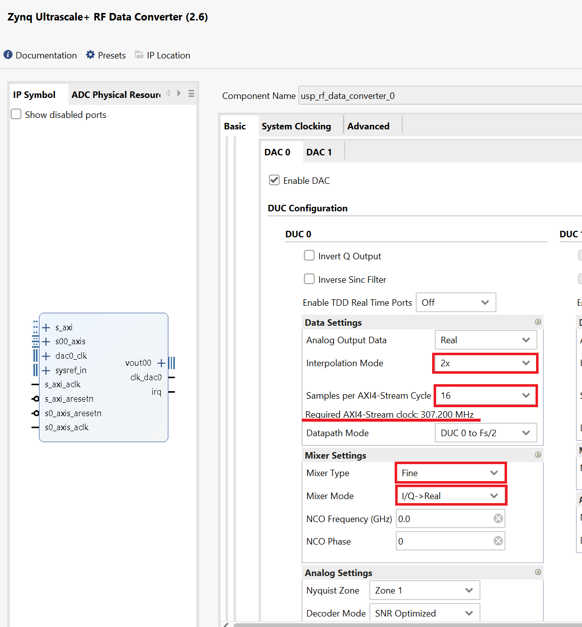
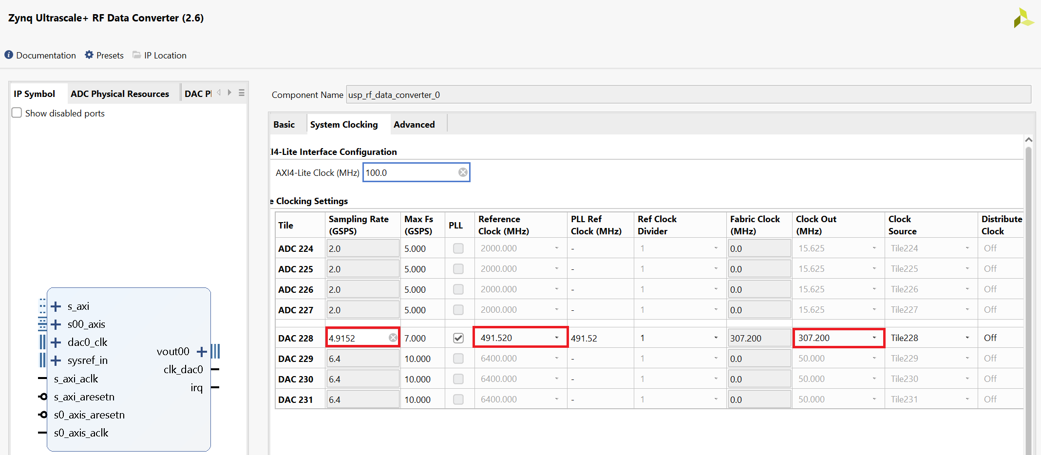
I’m including some screenshots of settings, but if there is a potential problem not shown in them, I’m including the .tcl file later in this post.

RF DC settings


MPSoC PL clock settings

Additionally, I had to modify the DMA read channel parameters so that the bus width matched my DAC AXIS input.

The software:

I have less confidence in my software design than in my hardware. In particular, I don’t know what lines I need to include to make the DAC receive and output the data that the DMA produces.

My current code is as follows and runs correctly up to the indicated position.

from pynq import Overlay, allocate, PL
import numpy as np

PL.reset()
ol = Overlay(‘dma_to_dac_wrapper.bit’)
dma = ol.axi_dma_0
dma_send = ol.axi_dma_0.sendchannel
dac = ol.usp_rf_data_converter_0

data_size = 1000
input_buffer = allocate(shape=(data_size,), dtype=np.uint32)
for i in range(data_size):

input_buffer[i] = np.random.randint(0, 2**14)

The code works correctly up until this point. In the DMA loopback ILA post linked above, when the DMA sends data, we have to be sure to prompt the DMA to receive the data so that the FIFO does not get filled and hang the code. I’m assuming a similar operation is needed for the DAC since I do see code hanging if I use dma_send.transfer() only, but I’m unsure of what that DAC-receiving code should be. I’ve tried both read() and write() commands that I see listed in the help() output, but I’ve yet to be successful with them.

while True:

dma_send.transfer(input_buffer)
# dac.read() # ??
# dac.write(?,?) # ??
dma_send.wait()

Assuming my hardware is correct, can anyone suggest what I might be missing from my code that will allow me to send a repeating output from DMA to DAC that will be observable on an oscilloscope?

Any help on what is surely my plethora of issues with my design would be deeply appreciated.

This zip contains the .tcl, .bit, .hwh, and .ipynb files that I’ve been working with.
DMA_to_DAC.zip (770.3 KB)

1 Like

Hi,
With the RFDC block (so the DAC part), there is no need for a read or write function. This block will directly send the content received from the DMA to the DAC for analog conversion, and it will also return the digital translation of what your ADC received.

Have you checked the provided notebooks with the provided overlay to understand how the DAC can be controlled?
Here is the notebook: (RFSoC-PYNQ/boards/RFSoC4x2/base/notebooks/rfdc/01_rf_dataconverter_introduction.ipynb at master · Xilinx/RFSoC-PYNQ · GitHub)

Which channel have you enabled? Is it the one of DAC 0 (as there are 2 DACs in a RFSoC4x2)?

What is the frequency of the analog signal created by your enabled DAC?

Hi matthew,

Thanks for the reply.
I’ve just gone back to review the notebook you linked, and compared against when I first looked at it a couple of months ago, I have a much better understanding of what it’s doing. The first thing that pops out at me is:

base.init_rf_clks()

After having seen code involving the xfrdc and xrfclk libraries (which I don’t understand well) from other sources, I developed a suspicion after first posting that I was missing some clock initialization. When I attempt this code with my overlay, I get this error.

ol.init_rf_clks()

AttributeError Traceback (most recent call last)
Input In [5], in <cell line: 1>()
----> 1 ol.init_rf_clks()

File /usr/local/share/pynq-venv/lib/python3.10/site-packages/pynq/overlay.py:363, in Overlay.getattr(self, key)

358 """Overload of __getattr__ to return a driver for an IP or
359 hierarchy. Throws an `RuntimeError` if the overlay is not loaded.
360 
361 """
362 if self.is_loaded():
--> 363     return getattr(self._ip_map, key)
364 else:
365     raise RuntimeError("Overlay not currently loaded")

File /usr/local/share/pynq-venv/lib/python3.10/site-packages/pynq/overlay.py:931, in _IPMap.getattr(self, key)

929 return mem
930 else:
→ 931 raise AttributeError(
932 “Could not find IP or hierarchy {} in overlay”.format(key)
933 )

AttributeError: Could not find IP or hierarchy init_rf_clks in overlay

My first thoughts on this error is that there’s an IP missing from my block design that will allow PYNQ to handle this code. When I dig into the block design (rebuilt from here) of the default base overlay in Vivado, I see all of the clocks that run into the RF Data Converter IP originate from top-level inputs like mine do.
Do I need to use some other method of clock initialization or does my block design need modification?

Also, while I was digging the the default base block design and the linked notebook, I saw calls like this:

base.radio.transmitter.channel[0].dac_block.MixerSettings[‘Freq’] = 900 # MHz

When I dig down into the base.radio.transmitter IP, I see modules channel_00 and channel_02, which each contain amplitude_controller modules. My understanding is that these controllers convert AXI data inputs to AXIS stream data outputs to send into the RFDC DAC AXIS input port. Since my design has the AXIS output of the DMA running directly into the AXIS input of the RFDC, I don’t need additional IP in the path to handle conversions, correct?

Moving on from the notebook, you asked, “Which channel have you enabled? Is it the one of DAC 0 (as there are 2 DACs in a RFSoC4x2)?
I’ve just opened my design and confirmed that I have DAC Tile 228, DAC 0 enabled. On the block design, this corresponds to input port s00_axis and output vout00 being active.

You asked, “What is the frequency of the analog signal created by your enabled DAC?
I’m not certain of exactly what value you’re asking for, here, so I’m going to list some items I’m seeing in my RFDC settings.

  • Required AXI4-Stream clock: 200.000 MHz
  • AXI4-Lite Clock: 100.0 MHz
  • DAC 228: Sampling Rate: 6.4 GSPS
  • DAC 228: Max Fs: 7.000 GSPS
  • DAC 228: Reference Clock: 400.000 MHz
  • DAC 228: Fabric Clock: 200.000 MHz
  • DAC 228: Clock Out: 50.000 MHz

I did just notice a clock net difference between my design and the default base overlay. I have no nets connected to the clk_dac0 output in my design, but the default base overlay loops that clock back around to the s0_axis_aclk input as shown below. Should my design be doing something similar?

about the getattr issue:
Do I need to use some other method of clock initialization or does my block design need modification?

How do you add your custom design on your RFSoC 4x2? Via the UART port or manually, by downloading the .bit and .hwh to the board?

For all of my designs, I have been manually uploading the .bit and .hwh to the board through the jupyter interface.

In which folder of the board have you put these two files? In
/usr/local/share/pynq-venv/lib/python3.10 (it was my version)/site-packages/pynq/overlays/ ?

Thanks for the ongoing replies, matthew.

For all of my test designs, I’m storing those two files alongside my notebooks. They currently live in the following directory, the contents of which are in the .zip I linked in my original post:

/home/xilinx/jupyter_notebooks/TestRuns_Shawn/DMA_3d_readToDac

The getattr error is linked to a python code overlay.py in the folder I mentioned.

Could you please try these next steps?

In your board, check the folder “overlays” in /usr/local/share/pynq-venv/lib/python3.10/site-packages/pynq/overlays/ . There should be a folder “base” with the base.bit and base.hwh inside. There are the files for the architecture provided by AMD.

If there is that folder, go back to /overlays/ and create a folder with the name of your bitstream (dma_to_dac_wrapper). In that folder put your custom .bit and .hwh. Also put copies of the python codes from the base folder, because these might be initialisation files that you were missing for ol.init_rf_clks(). Check these python copies for some names adaptation, like in init.py.

You can remove that folder if it did not work.
After that test, retry ol.init_rf_clks() and check if there are new errors or none.

@feezus the base overlay has a specialized Base class that wraps many of the peripherals and calls.

The init_rf_clks is defined here

@matthew hinted about this, however there’s no need to copy the base.py file, you can call the xrfclk.set_ref_clks() directly from your notebook or create a specialized class.

You will probably need to call the init_i2c method.

Mario

Thanks for your input, Mario.

I’m away from the lab today, but I’ll try these tomorrow. In the mean time, I’ve been considering the code you’ve mentioned:

xrfclk.set_ref_clks(lmk_freq=lmk_freq, lmx_freq=lmx_freq)

as I’m commonly seeing in RFSoC 4x2 examples, those two arguments are:

lmk_freq=245.76, lmx_freq=491.52

While I don’t understand why this is the case, I think it’s worth noting that LMX freq is exactly double that of the LMK freq.
I’ve examined the block diagram of the base overlay in Vivado with these values in mind. While I can’t find any clock domains corresponding to the 245.76 MHz LMK frequency, I see that the 491.52 MHz LMX freq feeds the dac0_clk port on the RF Data Converter ip. My design, though, requires 400.00 MHz on that port.

I’ve seen other posts on these forums that have discussed the LMK and LMX freqs and many of those posts involve the use of the TICS software. If I’m going to be using clock values other than the commonly-used 245.76 MHz and 491.52 MHz values, do I need to generate .txt files using TICS to place next to my .bit files, or can I simply include:

xrfclk.set_ref_clks(lmk_freq=200, lmx_freq=400) ?

Hi @feezus,

do I need to generate .txt files using TICS to place next to my .bit files

I’m not an expert on this board, but I think if you need to use a different frequency, you need to use TICS to generate the configuration files.

Mario

Hopefully, this will be the last time I post on these forums this Summer.

I’ve successfully observed DMA-to-DAC signals on my oscilloscope. @matthew and @marioruiz , thank you both very much for your help this week.

For anyone coming to this thread in the future, here’s what I had to change to solve my problems. The .bit, .hwh, .tcl, and .ipynb are here: DMA_to_DAC_working.zip (673.0 KB)

Hardware Adjustments

First, I made some changes to the DAC settings in the RF Data Converter IP. Regarding my non-default RF clock settings, I attempted to use TI’s Clock Design Tool to help determine parameters alongside TI’s TICS Pro software to configure my LMX and LMK clocks. I was ultimately unsuccessful with this route, so knowing that the configuration of the RF DC in the base overlay works with default clock values, I adjusted my RF DC’s settings to match those. I see now that I used “Fine” and “I/Q → Real”, which I believe is an incorrect match for the data I’m testing with. Switching to “Coarse” and “Real → Real” for mixer settings will reduce the Required AXI-4 Stream clock by half, but should still function correctly with the rest of my steps below.


I manually entered the Sampling Rate and selected the Reference Clock that matched the default LMX and LMK settings. I then selected a Clock Out that matched the required AXI-4 Stream Clock, since we can conveniently use the former to drive the latter.

My adjustments to the Data Settings of the RF DC changed the input bus width, so I had to adjust the DMA Data Width settings to match.

Since we’ll now be using the RF DC’s clk_dac0 to drive the AXI-4 Stream devices, the ZYNQ MPSoC’s fabric clocks can be reverted to their original settings to reduce power consumption.

With the changes to the clock sources, some IP and wiring adjustments needed to be made.


First, I removed all clock and reset nets from my design. Since the AXI-4 Stream devices are now using a different clock frequency than the rest of the devices, we have a new clock domain to account for, which requires an additional Processor System Reset IP. This IP, as well as all other AXIS clocks can all be driven by the RF DC’s clk_dac0 (purple in the above image). Block Automation and Connection Automation were used to connect the AXI reset, PL clock (orange), dac0_clk (blue) and AXIS resets (green).

Software Adjustments
After making the clocking adjustments to my hardware design, the required software changes were minor. Here’s the program, stripped of unnecessary code and with added lines in bold:

from pynq import Overlay, allocate, PL
import numpy as np
import xrfclk

PL.reset()
ol = Overlay(‘dma_to_dac_wrapper.bit’)

xrfclk.set_ref_clks(lmk_freq=245.76, lmx_freq=491.52)

dma_send = ol.axi_dma_0.sendchannel

data_size = 1000
input_buffer = allocate(shape=(data_size,), dtype=np.uint32)

for i in range(data_size):

# input_buffer[i] = 2**14
input_buffer[i] = np.random.randint(0, 2**14)

while True:

dma_send.transfer(input_buffer)
dma_send.wait()

del input_buffer

As I said up top, these changes resulted in successfully sending data from the DAC.

Thank you again to everyone that contributed. I appreciate your time greatly.

1 Like

Thank you @feezus for reporting back the solution. I marked your post as solved.