Designing an Overlay using Vivado Integrated Logic Analyzer (ILA)
In this series of blogs, I will cover how to use the Integrated Logic Analyzer (ILA) to debug your overlay. Instrumenting an ILA should be your last resort when it comes down to debugging.
Simulation and co-simulation are the best way to verify your design, although debugging in the actual hardware can be very useful.
The main reason for these series of blogs is to address some of the most common issues that are reported in the PYNQ forums, these are typically related to the DMA IP. These series of blogs assume expertise in overlay creation.
Another blog about using ILA on PYNQ was written by @Yangjie_Qi Using ILA to debug IP
Related Blogs
Connecting to the ILA using HW Server [Part 2]
Debugging Common DMA Issues [Part 3]
Using an ILA without Physical micro USB cable [Part 4]
Designing the Overlay
I am going to design a very simple overlay, DMA loopback, at the time of writing PYNQ 3.0.1 is the latest PYNQ version, and I will use Vivado 2022.1, which is the latest Vivado version officially supported by PYNQ. I will target PYNQ-Z2, although the steps are similar for other boards, you can find scripts for Zynq and MPSoC devices in the companion GitHub repository.
Please, refer to
for thorough discussion about the DMA IP and how to configure it.
I will start with a very simple design with just a DMA. You can use one of these scripts to generate the basic design:
-
Zynq boards scripts/1_0_zynq_dma_overlay.tcl
-
Zynq boards scripts/1_0_mpsoc_dma_overlay.tcl
All of the scripts used for this series of blogs can be found here github.com/mariodruiz/PYNQ_tutorials/ila

Note, there will be slight differences in the block design you see if you are using an MPSoC device. I am not covering nor mentioning these differences again.
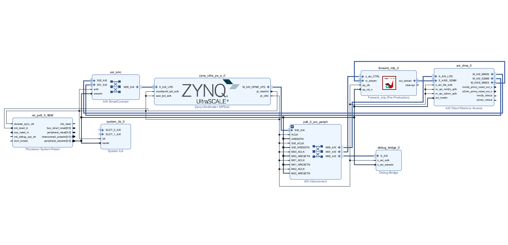
In this design, you can see that the AXI Direct Memory Access IP was added along a FIFO, in a sort of loopback design.
The next step is to add a System ILA IP and configure it with two AXI4-Stream probes.

Double click on the added System ILA IP to configure it. Set two interface slots and enable capture control (I like to enable this option)

Configure both SLOT0 and SLOT1 to be of interface type xilinx.com:interface:axis rtl:1.0

Connect:
-
system_ila_0/SLOT_0_AXIStoaxis_data_fifo/S_AXISpurple connection below -
system_ila_0/SLOT_1_AXIStoaxis_data_fifo/M_AXISpink connection below -
clock and reset
After this, you should have an overlay like this:

Verify and build your overlay.
Note: there are more ways of adding signals for debug. For more information, check out Using-the-System-ILA-IP-to-Debug-a-Block-Design
Download the Overlay
Connect to your PYNQ-Z2 board and move these files to the board.
-
*.bit: can be found in <proj_path>/<proj_name>.runs/impl_1/*.bit -
*.hwh: can be found in <proj_path>/<proj_name>.gen/sources_1/bd/<bd_name>/hw_handoff/*.hwh
Once you have the files in the board, create a new notebook. Or use the 1.dma_verification.ipynb
from pynq import Overlay, allocate
import numpy as np

ol = Overlay('dma.bit')
dma = ol.axi_dma
dma_send = ol.axi_dma.sendchannel
dma_recv = ol.axi_dma.recvchannel

data_size = 100

input_buffer = allocate(shape=(data_size,), dtype=np.uint32)
output_buffer = allocate(shape=(data_size,), dtype=np.uint32)

input_buffer[:] = np.arange(data_size, dtype=np.uint32)

print(f'Are buffers equal before DMA? {np.array_equal(output_buffer, input_buffer)}')

dma_send.transfer(input_buffer)
dma_recv.transfer(output_buffer)
dma_send.wait()
dma_recv.wait()

print(f'Are buffers equal after DMA? {np.array_equal(output_buffer, input_buffer)}')
After running this on the board, you should see that the buffers are equal after executing the DMA operation.
This concludes the first part of this blog series, see how to connect and use the System ILA
Please, use the comments section for questions related to the content of this blog. If you have questions about your own design or unrelated topics, please create a new topic in the forum.